Showing posts with label technology. Show all posts

Thursday, March 25, 2010

Flyfire

When I was an undergraduate at MIT in the late 1970s, one of the most impressive people I knew was my roommate Walter.

Walter was a mechanical engineer, and knew an incredible amount of just-plain-practical stuff about how to make things work, from types of stainless steel to the ins and outs of convective cooling.

The rest of us vicariously enjoyed his entry in Woodie Flowers' design completion, the 2.70 contest (named for the number of the design course). The idea was to take a box of stuff--tongue depressors, rubber bands, and so forth--and turn it into a machine that would beat other students in a glorified "king-of-the-hill" like task. This was way before I heard the phrase KISS, "Keep It Simple, Stupid," but we all learned that successful designs took this minimalist idea as a core principle.

This sort of contest has been picked up by others, even bringing high-school teams into the game, for example in the FIRST competitions. It's a great way to inspire imaginative people in ways that go way beyond the ordinary classroom experience. And it's a hands-on demonstration of the creativity that underlies true design.

Walter also worked with Otto Piene, the artist who headed MIT's Center for Advanced Visual Studies. Among other things Walter helped sew enormous inflatable anemones for Piene's Centerbeam project on the mall in Washington, D.C., as well as designing and building beam-steering mechanisms for an early laser show.

I'd forgotten all of this until reporting my latest story for CACM on a new project from MIT, which brings together two teams. One group comes from the Department of Urban Studies and Planning, which is exploring ways that distributed technology can illuminate or improve urban life, such as tracking trash disposal or using cell phones to monitor commuting. The second group is from the "Aero and Astro" department, where researchers have been exploring autonomous vehicles for military and other applications.

The Flyfire project aims to do something even stranger: to use LED-bearing helicopters to make a giant display. Although there may be some practical need for such a display, the most compelling vision for now is to create giant public art projects, of the kind pioneered by Piene and others.

Maybe it will never be particularly useful. Maybe it will never even work. But these grand visions tap into something essential in the human spirit.

Monday, March 1, 2010

Survival of the Most Entangled

Most people think quantum-mechanics affects only atomic-sized objects, but many experiments have shown that it applies over many miles. In an experiment last year, for example, researchers sent pairs of light particles, or photons, between two of the Canary Islands off the coast of Africa, a distance of 144 kilometers.


This picture dimly shows La Palma, where the photons started, as seen from Tenerife, where they were detected.

Although the Austrian team, led by Anton Zeilinger, only detected one in a million of the pairs they sent, they found that these pairs retained the critical property of entanglement. This means that results of measurements on the two particles are related in ways that can't be explained if each particle responds to the measurement independently: the pair acts like a single quantum-mechanical entity. Such pairs can be used to securely transmit information over long distances.

My latest story at Physical Review Focus describes a theoretical analysis of this experiment by researchers in Ukraine and Germany. They suggest that the pairs that survive the half-millisecond trip must have had unusually smooth sailing through the turbulent atmosphere, and that this is part of the reason why they are still entangled. (The motion of the air, like the shimmering of a mirage in the desert, generally disrupts the light transmission, but there are short moments of clarity.) This is a pretty comprehensible idea, so in the story I was able to sidestep a lot of interesting issues about how the entanglement was measured and what it means.

For example, the experimenters delayed one photon by about 50 ns by passing it through a fiber before sending it after the other one. That's not a long time, so the atmospheric conditions probably looked pretty similar to the two photons. Since they were subjected to much the same conditions, it doesn't seem so surprising that they would remain entangled. In fact, the original experimenters were pretty pleased that it all worked, but clearly they were hoping it might or they wouldn't have gone to the trouble.

Sending the two photons on the same path certainly isn't the most demanding task, either. More impressive would be sending them on different routes to a final destination where they were compared. But sending an entangled pair is good enough for some quantum communication schemes.

What made the paper particularly interesting was the conclusion that the turbulent atmosphere would be better than, say, an optical fiber that had the same average loss, because the fiber's properties wouldn't change with time. Zeilinger expressed pleasant surprise that the rare moments of exceptional clarity would more than make up for the times when the atmosphere was worse than usual. Still, having no turbulence at all (or a very clear fiber) would be even better.

Exploiting quantum mechanics in secure long-distance communication, for example via satellites, looks more realistic than ever.

Tuesday, January 12, 2010

Anniversary of Hopping Paper

Thursday, January 14, 2010 is the 25th anniversary of one of my first scientific papers, Hopping in Exponential Band Tails, in Physical Review Letters. It came out just as I arrived at Bell Labs.

It still surprises me that this paper has gotten nearly 200 citations, and that they continue to dribble in even now. Most papers are surpassed by new developments within a few years of publication. In this case, I stumbled on a useful but very accessible concept that people can easily wrap their head around. But I'd guess that most people that cite it have never read it.

The paper concerns motion of electrons in amorphous semiconductors, that is, semiconductors without a crystalline lattice. The best known example is the amorphous silicon alloys that are used for cheap solar cells.

Until the 1960s, some physicists questioned whether amorphous semiconductors could even exist (although they clearly did), because the quantum-mechanical understanding of semiconductors depended on the mathematical properties of wavelike electrons moving among the regularly-spaced atoms in a crystal. For electrons in some range of energies, the electron waves that diffract from the atoms destructively interfere, creating a bandgap with no electron states. At other energies, where there are electron states, they extend through the entire crystal. None of this mathematical framework for understanding semiconductors seemed to work unless the atoms were arranged in a regular crystal.

Phil Anderson, then at Bell Labs, showed in 1958 that if atoms were arranged in an irregular pattern, electronic states could exist, but be localized near particular atoms. Neville Mott and others suggested that in an amorphous semiconductors, electrons would be localized over some range of energies but extend infinite distances at higher or lower energies. The energies that separated the localized and extended states, which have the character of a phase transition, were called "mobility edges." If one conceptually replaces the band gap of crystalline semiconductors with the gap between mobility edges, then the mathematical treatment of amorphous semiconductors looks very familiar. Anderson and Mott shared the 1977 Physics Nobel with John van Vleck for their discoveries. Instead of being denigrated as "dirt physics," disorder is now a perennial topic in condensed matter physics

In Mark Kastner's group at MIT, we were studying what happened to optically generated electrons in the "band tails": the localized states near the mobility edge, whose number decreases exponentially into the gap. Based on some experiments I had done, I proposed that, at low temperatures, electrons would at first simply "hop" from one localized state to another, avoiding the extended states at the mobility edge altogether. Later on, as they moved to energies where the states where farther and farther apart, they would find it faster to hop up to where there were more states--but not all the way back to the mobility edge.

I called the energy to which electrons hopped--and where they could move easily--the "transport energy," and used a simple model to calculate how this energy varies with temperature.

If once conceptually replaces the band gap of crystalline semiconductors with the gap between transport energies, then the mathematical treatment of amorphous semiconductors looks very familiar. There are some important differences, though. For example, a magnetic field has a different effect on hopping electrons than on those that are freely moving. But although some details are different, the overall picture of amorphous semiconductors looks much like the pictures used by electrical engineers.

At the time, I was concerned that people would only remember Marc Kastner's name, so he graciously agreed to let me be sole author. I later regretted that selfishness, because anyone who knew Mark could see his style in it, and he certainly helped me to frame the ideas. Such are the follies of youth.

Monday, January 11, 2010

"World's First Molecular Transistor"


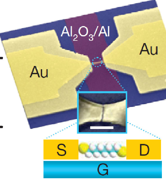
Overall electrode geometry, probably not for a device that was actually measured. Inset: Molecule-coated gold nanowire between the electrodes has developed a nanometer-scale gap because of electromigration, in which current pushes atoms away. White rectangle is 100nm long, for scale. Inset of inset: complete fantasy of what might happen in a small fraction of cases.

An interesting article in Nature, Observation of molecular orbital gating, got somewhat lost over the holidays, in spite of the breathless Yale University press release, Scientists create world's first molecular transistor.

Mark Reed of Yale and his colleagues made hundreds of small gold wires between large electrodes on a nominally 3nm-thick alumina insulator on a substrate and coated it with organic molecules. They then applied an electric current that pushed enough atoms out of the way to make a small gap in the wire. Near absolute zero, in a few of the wires, they then measured a current variation with source-drain voltage that looked like what they expected if the current was passing through a molecule close to the surface, whose energy they could change by applying a voltage to the substrate, or gate. In addition, to test whether the current was really going through the extra organic molecules, the researchers found sharp features in the current trace when the source-drain voltage brought the energy levels into alignment, in agreement with the molecules' "signature."

So far, so good. As the authors note, there have been previous observations of gated conduction in molecules before, but it's not easy to get two electrodes connected to a tiny molecule, let alone three.

But the press release says this shows that "a benzene molecule attached to gold contacts could behave just like a silicon transistor."

How does this fall short of that description? Let me count the ways.

No saturation. The current doesn't look at all like a normal silicon field-effect transistor (FET), where the gate voltage changes the channel resistance. Instead, the authors describe the conduction as tunneling between the two remaining pieces of the wire, while the gate voltage changes the precise energy levels in the molecule. The current is low near zero source-drain voltage and rises dramatically as the voltage increases. In contrast, the current in an ordinary FET rises linearly with voltage, like a resistor, and then saturates. In ordinary circuits, this saturation, corresponding to a voltage-independent current, is central to the transistor's gain, which gives it the ability to amplify power or to drive other transistors.

Low current. Tunneling conduction gives inherently low current levels. The currents observed are in the nanoamp range, a million or so times smaller than those in transistors on integrated circuits. This small current would take correspondingly longer to charge up any capacitor, so the circuits would be slow.

Large parasitic capacitance. Because the source and drain electrodes lie right on top of the gate, the actual capacitance is even bigger. Modern transistors are built with self-aligned processes that minimize the overlap capacitance.

Low gate coupling. The authors estimate that they need to put 4V on the gate to change the electron energies by 1V (25%). This is actually surprisingly good for a device like this, where multiplies of 0.1% are not unheard of. But it's still a problem. Silicon technologists work very hard to get perhaps 80-90% of the gate voltage to show up on the channel, and if it doesn't the device is very hard to turn off, resulting in excessive power. Moreover, if the energy isn't being controlled by the gate, it should be controlled by the drain, which means that it will never be possible to saturate the current to isolate the input from the output.

Packing Density. The entire device is much bigger than the molecule. From the micrograph, the electrodes are many microns in size. No doubt the electrodes could be made more compact, but to compete with integrated circuits they would have to be packed to separations comparable to their size, and this technique doesn't look like it could ever do that. No one really cares whether transistors are small. They care if they can be packed densely (and are cheap and fast and use little power).

Low Yield. The authors measured 35 devices that did what they hoped, out of 418 attempts, so about 8% of them worked. In contrast, in an integrated circuit only about 0.000001% of the transistors fail. (Or something like that--I don't have access to real numbers these days, but you get the idea.) Building a large circuit from occasionally-functional devices would require a completely new type of circuit design, and probably wouldn't be worth it.

This low yield is not surprising (or easily avoided), since the fabrication seems to demand that most of the current run through a molecule that is positioned right just at the gap and right at the corner where the wire meets the substrate, and that it not get blown away during the electromigration. Still, it is a matter of concern that devices are defined to be working if they do what the experimenters think they ought to do. This is a problem with many molecular fabrications schemes, and I give the team credit for doing the "inelastic tunneling spectroscopy" to verify the molecules have something to do with the current. But I would feel better if they gave an indication of how representative the devices they showed are.

The authors did a couple of other tests that I'm guessing didn't work as dramatically as they had hoped. First, they saw rather small differences between "insulating" molecules--fully saturated alkanes sandwiched between sulfur groups-- and "metallic" molecules--in which the organic "meat" of the sandwich is an aromatic benzene ring. Second, the voltage "fingerprints" of the molecules didn't shift when they applied the gate voltage, as one would naively have expected. The shapes and sizes of the peaks changed, but not their positions.

Overall, this is a nice research result, with some strong observations and some puzzling features. Some of my quibbles could be addressed in time, but it's not clear that these molecules will ever behave "just like a silicon transistor."

In 1997, Mark Reed was quoted to the effect that silicon technologists were "shaking in their boots" over his team's results. Those of us working in silicon technology at the time got a good laugh out of that claim, and went back to work. The new press release says that "Reed stressed that this is strictly a scientific breakthrough and that practical applications such as smaller and faster 'molecular computers'—if possible at all—are many decades away. 'We're not about to create the next generation of integrated circuits,' he said."

He's got that right.

Monday, December 14, 2009

Rules to Design By

Once something gets really too complicated, it's almost certain to fail. So how can computer chips, with their billions of components, work at all?

We know lots of other complicated systems, like the world economy or our own bodies. And we know those systems fail often dramatically or tragically.

Of course, computers fail, too, as you know if you've seen a "blue screen of death" recently. But although it won't make you feel any better, those crashes almost always arise from problems with the software, not the hardware it runs on.

So how do engineers ensure that integrated circuits, diced by the score from semiconductor wafers, have a very good chance of working?

Design rules.

Simply put, design rules are a contract between the engineers designing the process for making chips and the engineers designing circuits to put on them. The process engineers guarantee that, if the circuit designers follow these rules in the geometry of their circuits, the chips will work (most of the time).

You may have heard "minimum design rule" used as a shorthand to describe a particular "generation" of computer chips, such as the "32nm" technology recently introduced by Intel. But that is shorthand is somewhat misleading.

For one thing, the true gate length of the transistor--which is critical to their speed and power--is generally about half the generation name. In addition, the "coded" gate length--the length in computer-aided-design files--is not usually the smallest design rule. And this is just one of hundreds of rules that are required to define a technology.

Rather than dive into the details of transistor geometry, consider a simpler design rule: the minimum width of a metal wire connecting the transistors. Together with the spacing between the wires, this dimension determines how tightly the wiring can be packed, which for some circuits determines how many transistors can be used in a parcel of semiconductor real estate.

The minimum safe design width of a wire depends on how fine it can be made and still assure that it will conduct electricity. This has to be guaranteed even under variations over time of the process used to make it, as well as the variation in that process across a, say, 12-inch diameter wafer.

To test what number is safe, the process engineers will make a whole series of test patterns, each consisting of very long wires with various design widths. After measuring hundreds of these test structures, they have a good idea what they can reliably make.

In developing the process technology, they have hundreds of test structures, each aimed at testing one or more design rules. The structures are automatically measured on different positions on different wafers made in different processing runs. Only then will the engineers have the confidence to guarantee that any circuit that follows those rules will work.

After a long process, a set of design rules will be given to designers to use for their circuit layouts. None of this would work without computers to check whether a particular chip layout meets the rules, since the job is beyond human capacity. Therefore a key feature of the design rules is that they can be embodied in an efficient algorithm.

The design-rule paradigm has been extraordinarily successful. But its success depends on a characteristic of the failures it is intended to prevent: they are all dependent on the local properties of the circuit. Some of the more complex rules involve quantities like the area of the metal "antenna" that is connected to a particular device at some point during processing. And frequently the engineers will play it safe by crafting the rules to cover the worst possible situation. But if the rules are chosen and followed properly, there is no chance for a combination of small choices that satisfy the rules to join together to cause a problem in the larger circuit. That's what makes a chip with a billion transistors possible.


Wednesday, November 25, 2009

Green Computing

Supercomputers run the vast simulations that help us to better predict climate change--but they also contribute to it through their energy consumption.

The lifetime cost of powering supercomputers and data centers is now surpassing the cost of buying the machines in the first place. Computers, small, medium, and large, have become a significant fraction of energy consumption in developed countries. And although the authors of Superfreakonomics may not understand it, the carbon dioxide used to supply this energy will absorb, during its time in the atmosphere, some 100,000 times more heat energy than that.

To draw attention to this issue, for the last two years researchers at Virginia Tech have been reordering the Top500 list of the fastest supercomputers, ranking them according their energy efficiency in the Top Green500 list. I have a wee news story out today on the newest list, released last Thursday, on the web site of the Communications of the Association for Computing Machinery. The top-ranked systems are from the QPACE project in Germany, and are designed for quantum chromodynamics calculations.

Calculating efficiency isn't as straightforward as it sounds. The most obvious metric is the number of operations you get for a certain amount of energy. This is essentially what Green500 measures in its MFLOPS/W, since MFLOPS is millions of floating-point operations per second and watts is joules per second.

As a rule, however, this metric favors smaller systems. It also favors slower operation, which is not what people want from their supercomputers. Some of the performance lost by running slowly can be recovered by doing many operations in parallel, but this requires more hardware. For these reasons, the most efficient systems aren't supercomputers at all. The Green500 list works because they only include the powerhouse machines from the Top500 list, which puts a floor on how slowly the competing machines can go.

Over the years, researchers have explored a family of other metrics, where the energy per operation is multiplied by some power of the delay per operation: EDn. But although these measures may approximately capture the real tradeoffs that systems designers make, none has the compelling simplicity of the MFLOPS/W metric. This measure also leverages the fact that supercomputer makers already measure the computational power to get on the Top500 list, so all they need to do extra is measure the electrical power in a prescribed way.

These systems derive much of their energy efficiency from the processor chips they use. The top systems in the current list all use a special version of IBM's cell processor, for example. I worked on power reduction in integrated circuits more than a decade ago--an eternity in an industry governed by Moore's Law--and some of my work appeared in a talk at the 1995 International Electron Devices Meeting. I also served for several years on the organizing committee of the International Symposium on Low Power Electronics and Design, but I'm sure the issues have advanced a lot since then.

In addition to the chips, the overall system design makes a big difference. The QPACE machine, for example, serves up as about half again as many MFLOPS/W as its closest competitor by using novel water-cooling techniques and fine-tuning the processor voltages, among other things. These improvements aren't driven just by ecological awareness, but by economics.

There's still lots of room for improvement in the energy efficiency of computers. I expect that the techniques developed for these Cadillac systems will end up helping much more common servers to do their job with less energy.

Sunday, October 25, 2009

Reliability

A light bulb, floating over someone's head, has become a universal icon for a flash of insight. But the history of the incandescent bulb also shows that a good idea is not enough. The success of a new gadget often hinges on its ability to survive the rigors of the real world.

An electric current causes many materials to glow…momentarily. Glowing is a natural consequence of the "red-hot" temperatures produced by the current. But another consequence is reaction with oxygen in the air that promptly burns up the would-be filament. Protecting it in an air-free glass bulb is a key step toward practical electric light.

The filament material is also critical. The recently reopened Thomas Edison National Historical Site in West Orange, New Jersey recounts Edison's 1870s search through thousands of candidates, many involving carbonized threads of various sorts, including exotic materials like bamboo. Much of this selection process aimed at increasing the lifetime beyond the 15 or so hours of the first "successes." (British inventor Joseph Swan devised a similar device in Britain around the same time.)

Some 25 years later, Hungarian and Croatian inventors introduced the tungsten filaments like those we we use today, which last longer while providing more light.

The tungsten-halogen lamp extends the improvement. Its white-hot filament delivers much more light in the visible part of the spectrum, but over time even tungsten evaporates at these temperatures. Small amounts of halogens like iodine or bromine in the bulb react with the evaporated tungsten. The resulting halide migrates back to the filament where the heat decomposes it, leaving the tungsten back where it started, while the halogen goes on to pick up other stray atoms of tungsten. The result is a brighter, more efficient bulb.

Situations like this, where performance is directly improved by increasing the lifetime, occur frequently, for example in semiconductor electronics. In one example that I encountered while working in integrated-circuit technology a decade ago, making a transistor shorter improves its speed, both by increasing the electric field and by decreasing the distance electrons have to traverse. But a few of the more-energetic electrons cause atomic rearrangements that build up over time to change the transistor's properties and render it useless. The shortness of many transistors, and thus their performance, was directly limited by the need to avoid these "hot-electron effects."

The study of processes that lead to eventual failure goes by the somewhat misleading name of reliability. Typically, after an initially high failure rate, called "infant mortality," a batch of devices settles into a steady, low failure rate over time until some accumulating damage leads to eventual wearing out of all of the remaining devices.

Experiments on many similar devices are required to get a complete picture of the different ways they fail. Researchers need to know not just the median lifetime but its statistical distribution, to place strict limits on the number of possible failures. The statistics are also needed to guarantee that a complex circuit with many devices will continue to function.

Reliability engineers also need to quickly measure degradation with accelerated testing, for example at elevated temperature. They then extrapolate those results back to the milder conditions of ordinary wear and tear. For example, if you've owned your computer for a few years, its transistors have already been around much longer than the prototypes that were used to vet the latest manufacturing changes.

Confidently extrapolating wear-out times requires deep and accurate models of subtle, microscopic degradation mechanisms. As a result, reliability involves many fascinating physical phenomena, as well as an appreciation of statistics and of the ways that devices are put to practical use.

And as it does for the light bulb, this understanding can improve performance just as profoundly as a new invention can.


Saturday, October 17, 2009

What's In a Name?

I was surprised to see a fresh flurry of news stories in the last few days, more than a month and a half after two papers about ostensible magnetic monopoles in spin ices were posted online (although they just came out in print.)

I want to say one word to you. Just one word.

Are you listening?

Magnetricity.

Apparently one of the teams behind the monopole experiments has a new letter to Nature (with an accompanying News and Views article) measuring the total magnetic "charge" in a model-independent way using muons. (See the lifted graphic for a little explanation.)

The researchers adapted a venerable technique for measuring the charges of ions in electrolyte solutions. In a magnetic field, opposite monopoles drift in opposite directions, and the muons sense the field that results from their separation. Seems like a nice experiment.

But by calling the effect "magnetricity," the scientists insured themselves breathless coverage. It's great marketing, although as far as I can tell they did not measure the magnetic analog of an electric current as claimed by some news stories. They measured the separation that results from the current, but not the current itself.

According to the news release,

Dr Sean Giblin, instrument scientist at ISIS and co-author of the paper, added: "The results were astounding, using muons at ISIS we are finally able to confirm that magnetic charge really is conducted through certain materials at certain temperatures – just like the way ions conduct electricity in water."

Now you might not think that the lethargic drifting of magnetic "charges" that only exist in a very special crystal would form the basis of a new information technology, especially when you realize that "certain temperatures" are about a degree above absolute zero. After all, drifting electric charges in electrolytes (like batteries) are only important because they liberate truly mobile electrons in attached wires that do the real work.

But for researchers who only last month claimed to discover a fundamental particle predicted by Dirac, is revolutionizing electronics too much to ask? According to New Scientist,

Bramwell speculates that monopoles could one day be used as a much more compact form of memory than anything available today, given that the monopoles are only about the size of an atom.

"It is in the early stages, but who knows what the applications of magnetricity could be in 100 years time," he says.

I think I might be able to guess.

[Other stories at Physics World(the best one I saw), The Times, BBC, (did I mention the researchers were from the U.K.?), Popular Science, and Next Big Future.]

Thursday, October 8, 2009

Are the Nobel Categories Obsolete?

Considering that they've been around for more than a century, the Nobel science categories of "physics," "chemistry," and "physiology or medicine" have held up pretty well. But in truth, much of their durability reflects the fact that the committee hasn't worried much about their precise definitions. Nor have they paid much attention to Alfred Nobel's requirement that the prizes go to "those who, during the preceding year, shall have conferred the greatest benefit on mankind." (Care to make a case for the cosmic microwave background, anyone, other than that understanding the universe is inherently "beneficial" to mankind?)

Still, as noted by Doug Natelson, some people will regard this year's physics prize as an injustice, because both the fiber and CCD achievements are primarily engineering, not physics. In fact, both Kao (with processing experts from Corning and Bell Labs) and Boyle and Smith had previously gotten the Draper Prize, which is often described as the "Nobel Prize of Engineering," as had 2000 Physics Nobel Laureate Jack Kilby, one of the inventors of the integrated circuit (William Noyce had died by the time of the Nobel).

The conflation of physics and engineering raises two issues. On the one hand, some physicists will justifiably ask what right the Nobel Committee has to give their prize to people who aren't even doing real physics. I partially agree with Doug that this is an elitist attitude that devalues the real intellectual contributions of engineers. But what Kao did was engineering and materials science, and what Boyle and Smith did was electrical engineering. That doesn't mean it's inferior. It just doesn't happen to be physics.

On the other hand, some engineers will justifiably ask what right the Nobel Committee has to give credit to physics for accomplishments that were made by engineers. This sort of award reinforces the conceit that any transformative technologies must derive from basic science. The reality is that many of the technologies that are changing our world, like google or Wikipedia or eBay or iPhones or even cell-phone cameras, have little need for fundamentally new science--they rest on clever, imaginative, solid engineering.

The other science prizes have an even bigger mismatch, but for them it reflects the excitement and importance of biology, which has no prize of its own. "Physiology or Medicine," for example, has long been dominated by fundamental biology, which more and more relies on molecular biology. This trend leads to a collision with the "Chemistry" prize, which has also been increasingly dominated by molecular biology (not even biochemistry, really). Many prizes might fit equally well in either category, while other exciting fields are left out entirely.

The growing number of category-defying prizes reflects the reality that many exciting discoveries today lie between disciplines or in collaborations between disciplines, as the chemists, physicists, electrical engineers, materials scientists, biologists, and others who contribute to "nanotechnology" can attest. At the same time, some mature areas of physics and chemistry have really solved most of their interesting problems. Their practitioners have valuable skills and insights, but their traditional topics may not be offering the interesting challenges they did in the past. The Nobel categories are only a symptom of a larger issue in academic research that rewards research that fits with centuries-old disciplines.

The Last Ten Physics Nobels (Bold indicates those that are arguably engineering)

The Last Ten Chemistry Nobels (Bold indicates those that are arguably biology)

Tuesday, October 6, 2009

Optical Fiber

One half of the 2009 Nobel Prize in Physics goes to Charles Kao for his contributions to the development of low-loss optical fiber.

Although free-space transmission had been proposed by Alexander Graham Bell (and such optical techniques as smoke signals and mirrors were used for communication even earlier) optical signals did not become technologically important until the 1970s. The laser provided the needed bright light source, but sending light beams through the air or evacuated tubes never became widespread. Optical fiber, by avoiding the natural spreading of the beams and by letting them be routed like electrical signals in a wire, made widespread optical communication, including undersea transmission, possible.

Many researchers contributed to the development of practical fiber. Early studies had demonstrated the principles of total internal reflection that allowed light to be guided down gently curving paths, and the usefulness of an outer cladding to keep light from leaking out into the surroundings. But in the late 1960s, the attenuation in optical fibers would have prevented signals from being sent more than a few tens of meters.

Charles Kao helped to elucidate intrinsic loss mechanisms in silica (SiO2) fibers. Inherent density fluctuations in the fiber cause Rayleigh scattering, which increases for higher-frequency light (which is why the sky looks blue and the setting sun looks red). On the other side, low-frequency light is directly absorbed by atomic vibrations in the material. The best transmission occurs for intermediate frequencies where each of these processes is relatively unimportant, which for silica is in the near infrared region of the spectrum. If impurities could be removed from silica fibers, Kao showed, this material could be much clearer.

A major advance came from researchers at Corning, who in 1970 made very clear fibers using chemical-vapor deposition from very pure ingredients. This technique lowered the loss to a few dB per kilometer, making long-distance transmission feasible. Bell Labs later developed a modified deposition process that further reduced the loss from tiny amounts of residual hydrogen in the fibers. Previous prizes, like the Draper Prize, have often included the Corning and Bell Labs contributions to making fiber communication practical. Modern fibers have losses of around 0.2dB per kilometer, meaning that a very useful 1% of the original light power will travel 500km down the fiber, an astonishing degree of clarity for a solid material.

Researchers have explored many variations on the silica fiber over the years. For example, a single crystal core might reduce density fluctuations, while avoiding a material without oxygen would have fewer high-energy vibrations and less absorption. Cheaper materials like plastic can make useful fibers for carrying light over a few meters. But for long-distance transmission, no material has displaced the silica that was championed by Charles Kao.

Charge-Coupled Image Sensors

One half of the 2009 Nobel Prize in Physics is shared by Willard Boyle and George Smith for the charge-coupled device (CCD) image sensor. Smith says they invented the CCD in 1969 at Bell Labs in Murray Hill, New Jersey, to give their semiconductor device organization leverage against a competing organization's magnetic bubble technology. (In a bit of Bell Labs dirty laundry, Gene Gordon says in this 2000 interview that he was originally listed with Boyle and Smith on the patent, and that he "never could understand why Bill Boyle was listed.") Although the magnetic technology never became important, the CCD became the mainstay of digital imaging for decades.

Electronic devices detect light when it liberates electrons, either into vacuum (as in a photomultiplier) or within a semiconductor. A key challenge is that these photogenerated electrons must outnumber the background "dark current." This becomes more difficult when light levels are low, as in many scientific experiments, or when individual pixels are made small so that they receive few photons. The CCD addresses this problem by electrically isolating the light-detecting region of the semiconductor from the detection circuitry, so it can accumulate electrons for seconds or longer if necessary. To read out the accumulated charge, the device uses a "bucket brigade" that efficiently passes the charge from detector to detector along a row. Circuitry at the end of the row measures the charge from each "bucket" in sequence as it arrives.

Since its invention, CCD technology has been used in thousands of scientific experiments, and it helped to establish the consumer digital camera industry. In the past decade or so, however, technologists have developed imagers based on the mainstream CMOS (complementary metal-oxide-semiconductor) technology by improving both the device design and the manufacturing process. These CMOS imagers are cheaper and can be integrated onto a single chip with the processing electronics, for which CMOS is standard. CCD technology is still preferred for the highest quality images and the lowest light levels, such as those in the Hubble space telescope.

Over the years, researchers have considered CCD technology as a replacement for CMOS in low-power electronics, but it has not had wide impact in that application.

Monday, September 28, 2009

We Did All We Could

As you read this on your computer screen, it's easy to take for granted the billions of transistors--driving the screen, running the programs, storing the data, and bringing it to you over the internet--that make it all possible.

This embarrassment of transistors is affordable because they're made in a parallel process that produces vast numbers of similar devices at once, combined into integrated circuits (ICs). Making sure that they each behave the way they're supposed to demands extraordinarily clean and reproducible manufacturing processes. In fact, after inventing the transistor, Bell Labs was late to the IC party because they didn't think anybody could get them all to work at once.

Later, Bell Labs' parent, AT&T, did get good at ICs. Towards the end of my time in semiconductor device research at Bell Labs I worked with the excellent developers of the upcoming integrated circuit generations for what was then AT&T Microelectronics, who had moved to Orlando, Florida.

One benefit of visiting Orlando and learning about their challenges was that I managed to design some test structures that they included on the photomasks they used to develop their process. It took some convincing for them give up even a tiny piece (about 0.002 square centimeters!) of their very precious real estate. They also need to be sure that my devices wouldn't flake off and mess up other structures that they needed to do their real work.

Months later, it was a real rush to get the first silicon wafers with my devices on them.

First, the structures looked exactly like what I designed. Instead of looking at multicolored rectangles in a CAD program on a computer screen, though, I was looking at multicolored rectangles in a microscope: real semiconductor devices.

Second, there were lots of them. Even though the entire array of test structures was over a square centimeter in area, there were dozens of repetitions on each eight-inch-diameter silicon wafer.

Third, they were all the same. They didn't just look the same: on the unfortunate occasions when I blew one up with too much voltage, I learned that its repeated version would have very much the same electrical behavior.

I also made friends with people who did testing, robotically stepping across the wafer to measure each repetition. So for simple measurements, after a lot of up-front planning, I could sit back and let the data roll in. Whenever development ran a lot of 25 wafers through the several hundred steps it took to get finished ICs, they also made me hundreds of test structures, and measured them, too.

Compared to what I was used to in the physics labs, where you might work weeks to get a sample or two, this was heaven.

With lots of people helping out, we also did something more challenging, which was to explore new ways to process the wafers. For example, my research colleague Joze Bevk devised a scheme to improve the addition of electrical dopants into the narrow poly-crystalline-silicon ribs that formed the gates of the transistors. Our development colleagues helped track the wafers through step after step of the modified process.

One day, when Joze and I were visiting Orlando, our colleague Steve Kuehne approached us. In the matter of a surgeon telling waiting relatives "I'm sorry. We did all we could," Steve gave us the bad news: "The gates are falling off." Joze and I were very disappointed at this failure, since from Steve's grave expression it was clear that the result was a disaster.

Over the next hour or so, as we discussed what sort of stresses in the materials might cause these terrible problems, an interesting fact emerged. Out of many millions of gates on the test wafer, perhaps 20 had fallen off! Only the high-throughput measurement tools in the development line, which scan the entire wafer looking for anomalies, could even detect them. This is what Steve meant when he said the gates were falling off. For him, a process with even that many broken devices was a non-starter.

I don't doubt that the developers could have devised modifications of the process that reduced the problem, it if had seemed worthwhile--or if they had invented it themselves. Nonetheless, it was a powerful reminder of the degree of reproducibility that IC manufacturing demands.

When I see a news story about some new technique that's going to change the way ICs are made (like this one or this one--not to pick on IBM), I remember how few failures are deadly. If you can see variation in a handful of devices, then someone is going to have to do an awful lot of work before they can be made by the billions.

Now go back to taking them for granted.

Monday, September 21, 2009

Photo Finish for the Netflix Prize

It's not every day you see seven computer scientists grinning awkwardly behind one of those goofy six-foot checks they give out to lottery winners.

That was the scene in Manhattan's Four Seasons Hotel this morning as Netflix announced the winners of their $1 million competition to improve the system that underlies the movie recommendations that they make to their customers. I wrote about these "recommender systems" and the Netflix Prize in the August issue of Communications of the Association for Computing Machinery. Just as that article was going to press, someone beat the 10%-improvement threshold for bringing home the award.

But only today did Netflix announce that the winning team was BellKor's Pragmatic Chaos, a longtime leader, some of whose members appeared in my story. Although this team was the first to break the barrier in late June, other teams had subsequently passed them, and they submitted their winning entry only 20 minutes before the deadline (30 days after the barrier breaking). In fact, another submission matched their 10.6% improvement --but because the Ensemble team submitted their entry ten minutes later, they spent the presentation clapping politely from the audience.

Most researchers will say the prize money is only a part of the excitement of this competition--and in any case the winning members from AT&T Labs will be handing their winnings over to their corporate sponsor. A major draw for researchers was access to Netflix's enormous database of real-world data. The company also maintained an academic flavor by requiring that winners publish their findings in the open literature, and by maintaining a discussion board where competitors discussed results and strategy.

We don't know how many other companies have taken advantage of these open results, but Netflix certainly has. Netflix's Chief Product Officer Neil Hunt says the company said the company has already incorporated the two or three most effective algorithms from the interim "progress prizes." Moreover, "we've measured a retention improvement" among customers, Hunt said. The company is still evaluating which of the several hundred algorithms that were blended together to win the prize will be incorporated into future recommendations, since the results need to be generated very rapidly. "We still have to assess the complexity of introducing additional algorithms," Hunt said.

At the ceremony, the company didn't talk much about the other features, beyond predicting "star" rankings, that define good recommendation systems. As discussed in my CACM story, these include aspects of the user interface, such as the way users are encouraged to enter data and the way the results are presented. In addition, a good recommendation needs to go beyond predictable satisfaction to include serendipitous choices that a customer would not find on their own.

Rather than take on these more psychological challenges, the "Second Netflix Prize" will address the more algorithmic challenge of making predictions for customers who haven't ranked many movies, for example those who just signed up or who don't feel like providing ratings. To augment this "sparse" data, Netflix will provide competitors with various other tidbits of data, including demographic information like zip code and data about prior movie orders. But not, Hunt hastened to add, names or credit-card numbers.

As my earlier story discussed, such "implicit" user information is of growing importance for recommender systems. For one thing, it's harder to distort this kind of input by pumping up certain products with fake ratings. In addition, although Netflix can easily cajole customers to take the time to enter ratings, many commercial sites are more limited and have only implicit data to work with.

The new prize doesn't set any explicit performance goals. Instead, Netflix plans to award $500,000 each to the best performers as or April, 2010 and April, 2011. But most of the winners today weren't sure they were going to sign on to the new challenge. They were too tired.

Monday, September 14, 2009

The First Transistor


Over the weekend I helped guide some residents of Berkeley Heights, New Jersey (my home town), through the museum at Bell Labs (which is also in the town, although its postal address is Murray Hill). The free, publicly accessible lobby exhibit is an amazing testament to the many contributions that Bell Labs has made over the decades.

My personal favorite display is a replica of the original transistor, which was created in this very building (in the center of this google maps picture) in late 1947. It is amazing to think that there are billions of these electrical switches in the laptop that I'm typing this on, which cost me a few hundred dollars.

What was funny about showing this replica to non-experts, though, is that they naturally perceive it the way they do the other devices on display, as the carefully crafted product of finely-honed technology. In fact, the thing is a complete kluge.

It's easy to miss the scientific centerpiece of the whole apparatus: it's the silvery-gray slab sitting on top of the larger copper-colored slab. This is the semiconductor, in this case a piece of very pure germanium, which you can only make out in the picture because of a reflection from its somewhat ragged edge. Semiconductors, with their ability to morph from a metal-like conductor to an insulator and back again, are the materials that make the entire electronics industry possible.

The other key ingredient that you can't see is at the bottom of the clear triangle. That triangle itself is just a piece of plastic or something. The trick is that the experimenters wrapped some gold foil along its edge (probably more sloppily than in this replica). At the tip of the triangle, they then sliced the foil with a razor blade to form a very narrow gap, probably tens of microns in width, between two remaining pieces of foil. They connected the two pieces to separate parts of their electric circuit with the thin coiled wires you can see.

They then smushed the tip of the triangle, with its two almost-touching pieces of gold foil, into the surface of the semiconductor. To hold it in place, they fashioned a spring from the stiff wire, maybe a paper clip, that you see in the replica The final step is to connect their circuit to the copper-colored block, and thus to the semiconductor. So most of what you see in the picture is just there in a supporting role. The two pieces of foil, each touching the semiconductor, and the tiny gap between them, is where all the action is.

For electricity to get from one piece of foil to the other, it has to pass through the semiconductor. Applying an electrical signal to the base that supports the semiconductor, changes its properties, changing the amount of current that flows. The result is that a small signal on the base turns into a big change in current, so the signal is amplified. Even then, the current has trouble making it very far, which is why the gap has to be small. One of the first things the researchers did was to connect it to a speaker (like those in the telephones of their employer, Ma Bell) and verify that, yes, it sounded louder.

This rickety contraption is a classic experiment in progress. In fact, I'm confident that, at first, the real thing looked a lot messier than this replica. The scientists were throwing stuff together to see whether they could see the transistor action. If this hadn't worked they'd have thrown something else together, maybe with a narrower gap or a different metal, or washed the semiconductor differently.

To me, the ugliness of this device is its beauty. It's a snapshot of a discovery in progress.


Recent history note: The replica in the picture, unlike the one in the museum, was made for a 50th anniversary celebration held at the Murray Hill facility in 1997. Lucent Technologies' Microelectronics Group, the name on the plaque, included both the integrated-circuit business and the optoelectronic-device businesses (not including optical fibers). Three years later, Lucent decided to spin that group off as Agere Systems, along with the people at Bell Labs (like me) whose work related to those businesses. (In a separate decision, they sold their optical fiber group and the associated Bell Labs members.) Within another few years, the optoelectronics business had been sold to Triquint, and much of it later became Cyoptics, while the IC business had been acquired by LSI. Most of the people from Bell Labs (like me) had already left. So it goes.

Tuesday, September 8, 2009

Memristors

One frustrating aspect of science writing is that there's little market for stories that are skeptical about a new advance, but there's a big market for stories that run with the hype.

One widely covered "beyond Moore's law" story last year was the announcement from HP Labs that they had discovered the "fourth basic circuit element," the "memristor," which "could transform computing." As I've complained before, lots of researchers think they can solve industry's problems even though they don't know what they are, but in this case I think the strategy is more deliberate.

HP, in fact, has a history of visionary claims. In 2005, for example, they announced the "crossbar latch": "Who Needs Transistors? HP Scientists Create New Computing Breakthrough at Molecular Scale." They described dense arrays of devices whose resistance depends on previous voltages. But their claims, such as their ability to "restore" signal levels, were quite misleading, since the depend on surrounding their structure with normal transistors. The devices themselves, although densely packed, were slow and passive and certainly not a threat to transistors.

In spite of this history, most news coverage of the memristor repeated the framing in the HP press release: this was the "fourth element" that researchers had sought for decades. U.C. Berkeley electrical engineering professor Leon Chua authoritatively endorsed this view.

Unfortunately, it was Chua who had made the original claim about the memristor, in a 1971 paper that was cited only about 20 times over the next 37 years. In reality, no researchers were beating down the bushes looking for this device; most had never heard of it. Meanwhile many experimenters, including those at HP, had made devices that had the special properties of memristors, but didn't need see a need for that language. Now the crossbar latch appears to contain memristors.

So what elite group is the memristor supposed to be the fourth member of? The other three members are the resistor, capacitor, and inductor. These are the passive, linear, two-terminal circuit elements found in every textbook. Passive means they don't provide power, and two-terminal means they just have two wires coming out. Linear means that output is proportional to input, but for reasons I'll explain below that word was left out of the HP descriptions.

In his 1971 paper, Chua argued that these elements relate either the current or its integral over time (the charge) to the voltage or its integral (which he somewhat surprisingly calls the magnetic flux). The resistance relates current to voltage. The capacitance relates the charge to the voltage. The inductance relates the current to the flux. And one thing is missing….

This unusual description of these familiar devices is a little unnerving. But as Chua modestly explains to Information Week:

"Electronic theorists have been using the wrong pair of variables all these years -- voltage and charge. The missing part of electronic theory was that the fundamental pair of variables is flux and charge," said Chua. "The situation is analogous to what is called "Aristotle's Law of Motion, which was wrong, because he said that force must be proportional to velocity. That misled people for 2000 years until Newton came along and pointed out that Aristotle was using the wrong variables. Newton said that force is proportional to acceleration -- the change in velocity. This is exactly the situation with electronic circuit theory today. All electronic text books have been teaching using the wrong variables -- voltage and charge--explaining away inaccuracies as anomalies. What they should have been teaching is the relationship between changes in voltage, or flux, and charge."

What seems to be missing is something that relates charge (the integral of the current) to flux (the integral of the voltage). He postulated, and HP says they found, this missing element, called the memristor.

But remember that omitted word "linear"? The device that is in the same club as the resistor, capacitor, and inductor would have, like them, a proportionality between the quantities it relates. This simple linear relationship is what makes these devices fundamental. And if the integral of the current is proportional to the integral of the voltage, then their derivatives, the current and voltage, are also proportional. In other words, in this linear case--the only case for which a memristor can legitimately join the ranks of the other three devices--"the memristor reduces to a linear time-invariant resistor," in Chua's own words.

So the memristor only exists, as a fundamental circuit element, when it is just a resistor.

Of course, there are nonlinear generalizations of all of these devices, and things get complicated really fast. And real devices aren't purely one device or another. Capacitors, have some series resistance and some leakage resistance, for example.

Still, maybe thinking in terms of a general, nonlinear "memristivity" makes some observations easier to understand. Even if it doesn't, people may discover some cool stuff by exploring this area. And to their credit, HP researchers seem to be seriously pursuing this, as exemplified by this September 1 Nano Letter. But there's an awful lot of noise and hype that makes it hard to get a bead on the real issues. Certainly the story is much more complex than, say, finding a missing element predicted to be at a particular spot in the periodic table. It's more like deciding that Pluto wasn't really a planet after all--and we know how complicated that story gets.

Once a story like this gets out there, though, unless it's so widespread that virtually everybody has heard of it, it's very hard to sell a story that tries to put it back in the bottle, or even to give it some perspective. (I've tried.)

After all, why would you want to put a lot of effort into understanding something that not worth learning about in the first place?

I'll bet you haven't even read this whole post.

Tuesday, September 1, 2009

The End is Near

In today's New York Times, John Markoff reports on the impending end of Moore's Law. It's a well-written story, but it's one that could have been told--and has been--many times before.

For example, there's nothing wrong with this statement:

"Increasingly, transistor manufacturers grapple with subatomic effects, like the tendency for electrons to "leak" across material boundaries. The leaking electrons make it more difficult to know when a transistor is in an on or off state, the information that makes electronic computing possible. They have also led to excess heat, the bane of the fastest computer chips."

Except that we were saying much the same thing a decade ago. (For example, see this paper of mine from 2000. Sorry the formatting is a little bizarre.) The International Technology Roadmap for Semiconductors, which is the industry's formal embodiment of Moore's Law, has been seriously evaluating possible successors for a decade as well.

It's nice to see IBM's Frances Ross featured in the story. She's a wonderful, imaginative scientist, whom I knew when she spent some time at Bell Labs. But she did make a goof here.

When we were preparing to announce our Vertical Replacement Gate transistor to the world in 1999 (we did an exclusive with the same John Markoff), Jack Hergenrother and I took some training in dealing with the media. It was a very interesting session, and one message was "never predict when the work will be commercially available." It has financial implications, and it's too easy to get wrong.

Frances is quoted (indirectly) making exactly that sort of prediction about the silicon nanowires she's growing in her electron microscope: "this technology…could be available commercially by 2012, she said."

Maybe IBM is seriously committed to this, but I suspect that if that projection were true, it wouldn't be coming from a fundamental researcher. More likely, the technology IBM is going to use for their chips in 2012 is already in serious development and making large circuits, not in a research lab. All the intervening time will be needed to get the bugs out of the process and make sure the devices can be made by the billions.

My suspicion is heightened by a later statement that "techniques must be developed to make them behave like semiconductors." That seems kind of important.

Actually, I think nanowires made of traditional semiconductors are quite interesting, not as flashy but perhaps more practical that carbon nanotubes. But commercialization in 2012 sounds kind of silly, at least for full-scale integrated circuits.

The one thing it's safe to say is that we're ten years closer to the end of Moore's Law than we were a decade ago. We have a slightly longer laundry list of candidates to take over, but no obvious path for getting them to the enormous scale of circuit needed to take on silicon. In 1998, I suggested that the alternatives might sneak in by taking a low-performance, disruptive path, but silicon just kept getting better (although clock speeds did max out). Exponentials being what they are, Moore's Law will have to end, and it's hard to imagine it going 20 more years, if that.

But the really interesting question of how it ends, and what, if anything, comes next, is still wide open.

Monday, August 31, 2009

A Shrinking Target

Last week, Business Week published a lament from business consultant Adrian Slywotzky about declining industrial research in the U.S., and what we could do about it. The decline is not a revelation, but he's right to wonder where future technological innovations will come from.

I do think he exaggerates in describing Bell Labs as "essentially gone." For example, he claims that Bell Labs had 30,000 employees in 2001 and has only 1000 today (disclosure: my wife is one of the latter). Certainly the labs shrank after the dot-com bubble--as did the company that pays for them. But the 30,000 number included tens of thousands of people doing advanced development aligned with business--certainly not the sort of basic researchers Slywotzky is worried about replacing. Even when I went there in 1985, the research area at Bell Labs was not much over 1000.

Still, no honest observer could deny that Bell Labs is not what it used to be. But I think Slywotzky neglects a critical cause for changes at Bell and other research labs: the moves of their corporate parents away from vertical integration.

Like Ford, which in the 1920s bought Amazon rubber plantations to assure a supply for tires, the AT&T that spawned Bell Labs did everything. At the low end, they drew their own copper wire and developed durable plastic materials for telephones. At the high end, they provided both local and long-distance service to millions of Americans. With this vertically integrated structure, research didn't have to worry too much about what part of the company their innovations might affect. If it affected technology, AT&T could take advantage of it.

Even the 1984 breakup of local and long-distance didn't change this integration. It did remove the monopoly subsidy for Bell Labs, a name that AT&T kept. But to the surprise of many, it was the part of Bell Labs funded by the still-monopoly local phone companies, renamed Bellcore, that quickly ran into trouble. Bell Labs, although it became more focused, continued to pursue speculative long-term--or infinite-term--research.

When AT&T spun off Lucent Technologies in 1995, it kept many math and computer researchers, but physical science research was left largely intact as part of Bell Labs in the new company. But the company no longer provided phone services. When Lucent decided to spin off Optical Fiber Solutions and Agere Systems in 2000, they no longer made fiber, lasers, or integrated circuits. Bell Labs physical scientists were discouraged from research that supported these technologies (making Hendrik Schön's orthogonal work seem much more attractive). These spinoffs transformed the formerly vertically integrated company.

With the increasingly narrow vertical scope of Lucent's business (now merged with Alcatel but covering much the same product space) Slywotzky's description of material physics and semiconductor research as having been Bell Labs' "last remaining areas of basic science," seems misguided. For one thing, Bell Labs is still researching such things as using semiconductor chips to process light, which is certainly as basic as the introduction of the graphical user interface by Xerox PARC that he cites. But it is hardly surprising that a lab would shift its focus over time toward things the company actually does.

Although the shift is not surprising, the lack of vertical integration is a bigger challenge for long-term research. By definition, revolutionary innovations don't match well with existing businesses, so they face huge barriers in an established company. But in a smaller company that is focused on only one tier of activity, it's even easier for research to miss the mark, raising the pressure to shorten the time horizon. No innovation in semiconductor device physics, however profound, is going to help the bottom line of a telecommunications equipment manufacturer. The narrower the company's focus, the harder it is to argue that research has a chance of helping it.

I suspect IBM's much more vertically integrated model--they still manufacture integrated circuits as well as providing services--has helped IBM research to survive after a near-death experience in the early 1990s. Just last week, they revealed a very cool image of the organic molecule pentacene (ironically, one that was also studied by Hendrik Schön).

But although Slywotzky overlooks an important contributor to the decline, I agree with him that the U.S. and the world need to explore new ways to encourage long-term research.


Thursday, August 13, 2009

Too Much Information

When I was mulling over a career change to science writing in 2003, I found myself in an electronics store near a couple of twenty-something guys looking over some new gadget or another. The way they tossed around words like "gigahertz" and "megabytes," it was distressingly clear that they had no clue of the awesome intellectual content that was embedded in the device they would spend a few tens of bucks for. My desire to reveal to them what they held so casually in their hands helped to push me onto my new path.

Ironically, I've hardly written since on what allows people to design and build gadgets in which billions of transistors to work reliably together at a cost of maybe $0.000001 each. I have written a few stories on isolated experiments on one-off devices that the researchers hope could someday transorm technology, even though most of those speculative devices will never find their way to your pocket. But the reality is, most people are happy to use the real technology with no understanding of how it works.

You might think it would be different in biology. After all, everybody has (or is?) a body. Everybody gets sick, or knows someone who has. But the sad truth is that the detailed mechanisms of biology, as intricate and wonderful as they are, are no more interesting to most readers than are the details of their iPod. Sure, something complicated is going on in there, but as long as it works, who cares? And if it doesn't work, how likely is an average person to be able to figure out what to do about it?

So the intricacies of signaling networks or RNA interference, like those of electron velocity saturation or speculative execution, are likely to be forever consigned to a nerdy backwater. But there are still technical issues that people should understand, and that they will want to understand when they have proper motivation and context.

At the highest levels, for example, technical details are directly relevant. You don't have to know anything about discrete cosine transforms to know that an over-compressed jpeg image develops square blocks and ghosts of sharp edges. You don't have to know about cross-linking in cell walls to know that antibiotics are effective against bacteria but not viruses. And more accurate understanding can have important consequences. Fewer people using antibiotics when they are useless would delay the development of resistance. The way we view the biological mechanisms of drug abuse or homosexuality changes how we regard our fellow human beings.

Even without practical importance, though, even fine-grained technical details can be philosophically profound. The DNA sequences that we share speak to a deep connection and common history among all living things. The hive mind of social insects gives us new ways to think about our societies--and our brains. These insights deserve to be part of our common culture. The challenge for a science writer is to communicate their essential significance without overwhelming readers with unnecessary details.


Wednesday, August 12, 2009

RSS Feeds

I'm always surprised, as I was again this weekend, when an otherwise web-savvy friend doesn't know about RSS feeds. I've been using them for more than five years to keep track of things on the web, and when a computer problem recently derailed them for a few days, I felt like I'd been blinded. (Okay, it was a bit of a vacation, too.) So here's my advertisement for RSS (which stands for something that is less important than the initials, like DNA).

I track over 200 feeds, including various blogs, local and national news sites, science magazines, news release sites, university labs, scientific journals, economics sites, and a couple just for fun. For me the key advantages over visiting the web page are first that it looks for new items automatically, but equally important that I don't have to read anything twice (with a few exceptions). Just as in an email program, items that haven't yet been viewed are bold, so it's easy to see what's new. The presentation also gives an easy drill-down capability, progressing from a headline, to a description, to a complete web page, which is a very efficient way to browse through items that are not all equally interesting.

I use the free aggregator FeedDemon, although there are others, and many browsers have RSS capability built in. FeedReader lets you organize feeds in folders, which I find useful because it helps me to predict how much time it's going to take by grouping similar sites. Sites like CNN that have lightweight news items can be scanned quickly, for example, whereas if you're going to take the trouble to look at a journal table contents you'd better be ready to spend some time. If I'm in a hurry, I flag items like journal articles or longer stories to return to when I have the time to spend.

If you monitor any web sites on a regular basis, you owe it to yourself to them with RSS. Download a reader or use a browser, and when you give it the URL for a site, it will most likely auto-discover the feed. You won't look back.

Tuesday, August 4, 2009

Other Customers Who Bought This Item…

My news story on recommender systems (subscription required) is in the August issue of Communications of the Association of Computing Machinery.

Even if you don't recognize the phrase, if you do much of anything on the web you've dealt with "recommender systems": they're the programs that let Amazon, L.L. Bean, YouTube, and pretty much everyone else offer "suggestions" about other items that might interest you.

The timing of this story turned out to be very good. A major driver for this field in the past couple of years has been the Netflix Prize, which offered a million dollar reward to a team that could beat, by 10%, Netflix's algorithm for predicting movie preferences. To lure researchers, the company offered access to its enormous database of customer preferences, but they stipulated that the winners must make their techniques publicly available. The openness of the competition has attracted thousands of competitors, and stories in Wired and the New York Times Magazine, and IEEE Spectrum. It's taken a while, and some researchers were even speculating that Netflix had some secret knowledge that 10% was unreachable, but in the last month a couple of different teams have finally inched past the goal. (As of this writing, the official winner hasn't yet been announced, though.)

What makes my story gratifying, though, is that it goes beyond the prize to put these systems in a larger context. The 10% goal is based on the typical (root-mean-square) discrepancy between the predictions and the actual preferences reported by customers in a secret test batch. But predicting things that people will like is only a beginning. What people really need is pleasant surprises--items that they wouldn't have found on their own. In many cases, this means that the most useful predictions must make mistakes. This is a different goal from that for traditional "classifiers" that trade off false positives with false negatives. (In October in New York, the ACM is sponsoring a conference devoted entirely to recommender systems.)

Another key issue is the user interface, including how data is gathered and how recommendations are presented. If Amazon tells you that customers who bought the glass tumbler you ordered "frequently bought" a pet nail grooming rotary tool (as described recently in Consumer Reports), it makes a funny story. If they told you that the pet tool was especially selected for you by their highly tuned software, you'd likely conclude they were delusional.

One of the fun applications is in music. As part of my "research" I tried out the internet radio station Pandora. I seeded the station with some of my quirkier art-rock music from the early 70s, like Gentle Giant, and was really blown away when it played other music from the distant corners of my collection that I didn't think anyone else new about. Interestingly, the Pandora team uses a large team of musicologists to classify tunes, and does not rely exclusively on user's preferences.

The million dollars that Netflix ponied up is a hint of how commercially important these systems are. Even when we're not aware of it, they will shape more and more of our technological experience, both on the web and with mobile devices. Stay tuned.