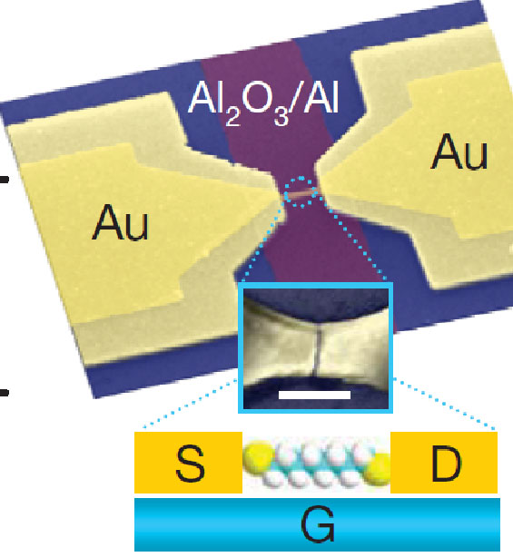
Overall electrode geometry, probably not for a device that was actually measured. Inset: Molecule-coated gold nanowire between the electrodes has developed a nanometer-scale gap because of electromigration, in which current pushes atoms away. White rectangle is 100nm long, for scale. Inset of inset: complete fantasy of what might happen in a small fraction of cases.
An interesting article in Nature, Observation of molecular orbital gating, got somewhat lost over the holidays, in spite of the breathless Yale University press release, Scientists create world's first molecular transistor.
Mark Reed of Yale and his colleagues made hundreds of small gold wires between large electrodes on a nominally 3nm-thick alumina insulator on a substrate and coated it with organic molecules. They then applied an electric current that pushed enough atoms out of the way to make a small gap in the wire. Near absolute zero, in a few of the wires, they then measured a current variation with source-drain voltage that looked like what they expected if the current was passing through a molecule close to the surface, whose energy they could change by applying a voltage to the substrate, or gate. In addition, to test whether the current was really going through the extra organic molecules, the researchers found sharp features in the current trace when the source-drain voltage brought the energy levels into alignment, in agreement with the molecules' "signature."
So far, so good. As the authors note, there have been previous observations of gated conduction in molecules before, but it's not easy to get two electrodes connected to a tiny molecule, let alone three.
But the press release says this shows that "a benzene molecule attached to gold contacts could behave just like a silicon transistor."
How does this fall short of that description? Let me count the ways.
No saturation. The current doesn't look at all like a normal silicon field-effect transistor (FET), where the gate voltage changes the channel resistance. Instead, the authors describe the conduction as tunneling between the two remaining pieces of the wire, while the gate voltage changes the precise energy levels in the molecule. The current is low near zero source-drain voltage and rises dramatically as the voltage increases. In contrast, the current in an ordinary FET rises linearly with voltage, like a resistor, and then saturates. In ordinary circuits, this saturation, corresponding to a voltage-independent current, is central to the transistor's gain, which gives it the ability to amplify power or to drive other transistors.
Low current. Tunneling conduction gives inherently low current levels. The currents observed are in the nanoamp range, a million or so times smaller than those in transistors on integrated circuits. This small current would take correspondingly longer to charge up any capacitor, so the circuits would be slow.
Large parasitic capacitance. Because the source and drain electrodes lie right on top of the gate, the actual capacitance is even bigger. Modern transistors are built with self-aligned processes that minimize the overlap capacitance.
Low gate coupling. The authors estimate that they need to put 4V on the gate to change the electron energies by 1V (25%). This is actually surprisingly good for a device like this, where multiplies of 0.1% are not unheard of. But it's still a problem. Silicon technologists work very hard to get perhaps 80-90% of the gate voltage to show up on the channel, and if it doesn't the device is very hard to turn off, resulting in excessive power. Moreover, if the energy isn't being controlled by the gate, it should be controlled by the drain, which means that it will never be possible to saturate the current to isolate the input from the output.
Packing Density. The entire device is much bigger than the molecule. From the micrograph, the electrodes are many microns in size. No doubt the electrodes could be made more compact, but to compete with integrated circuits they would have to be packed to separations comparable to their size, and this technique doesn't look like it could ever do that. No one really cares whether transistors are small. They care if they can be packed densely (and are cheap and fast and use little power).
Low Yield. The authors measured 35 devices that did what they hoped, out of 418 attempts, so about 8% of them worked. In contrast, in an integrated circuit only about 0.000001% of the transistors fail. (Or something like that--I don't have access to real numbers these days, but you get the idea.) Building a large circuit from occasionally-functional devices would require a completely new type of circuit design, and probably wouldn't be worth it.
This low yield is not surprising (or easily avoided), since the fabrication seems to demand that most of the current run through a molecule that is positioned right just at the gap and right at the corner where the wire meets the substrate, and that it not get blown away during the electromigration. Still, it is a matter of concern that devices are defined to be working if they do what the experimenters think they ought to do. This is a problem with many molecular fabrications schemes, and I give the team credit for doing the "inelastic tunneling spectroscopy" to verify the molecules have something to do with the current. But I would feel better if they gave an indication of how representative the devices they showed are.
The authors did a couple of other tests that I'm guessing didn't work as dramatically as they had hoped. First, they saw rather small differences between "insulating" molecules--fully saturated alkanes sandwiched between sulfur groups-- and "metallic" molecules--in which the organic "meat" of the sandwich is an aromatic benzene ring. Second, the voltage "fingerprints" of the molecules didn't shift when they applied the gate voltage, as one would naively have expected. The shapes and sizes of the peaks changed, but not their positions.
Overall, this is a nice research result, with some strong observations and some puzzling features. Some of my quibbles could be addressed in time, but it's not clear that these molecules will ever behave "just like a silicon transistor."
In 1997, Mark Reed was quoted to the effect that silicon technologists were "shaking in their boots" over his team's results. Those of us working in silicon technology at the time got a good laugh out of that claim, and went back to work. The new press release says that "Reed stressed that this is strictly a scientific breakthrough and that practical applications such as smaller and faster 'molecular computers'—if possible at all—are many decades away. 'We're not about to create the next generation of integrated circuits,' he said."
He's got that right.


Hi Don - What I don't really understand is how this is any different, in terms of physics, than the other single-molecule transistor work that's been done over the last decade. Sure, they have inexplicably good gate coupling (to be able to see any gating effect in alkane chains or benzene dithiol is something that no one else has been able to do). Still, what they're reporting is the gate modulated shifting of nonresonant molecular levels. This is *exactly* what was done by, e.g., Park et al. in their 2000 Nature paper. Indeed, Park et al. gated the level (in C60 in their case) all the way into resonance. (In alkanes, w/ a several eV HOMO-LUMO gap, that's not realistic.) It's an interesting (and in places quite surprising) piece of work, but calling it the first molecular transistor doesn't seem justified to me.
ReplyDeleteThanks, Doug.
ReplyDeleteThat didn't stop Discovery News from pumping it, although they do say it's a scientific not a technological discovery.
Was it just me who was surprised that there wasn't a bigger difference between the saturated and aromatic molecules?
No, it wasn't just you. The large gate coupling reported in the paper is extremely surprising, given the overall geometry of the electrodes. I wonder if there's some trick to getting just the right electrode shape so that the gate field actually gets to the molecule so efficiently.
ReplyDeleteAs someone who's had students see no gating at all on hundreds (if not thousands) of electromigrated junctions with alkanes, I would have been very interested to see whether bare tunnel junctions show any gating. Lateral oxide tunnel junctions can be gated: http://dx.doi.org/10.1088/0268-1242/13/8A/023
One more point. You wouldn't necessarily expect any gate-dependent shift of the inelastic tunneling features; those are usually thought to be governed by the ball-and-spring vibrational modes of the molecule, and ordinarily shouldn't do much w/ gate. We actually saw signs of something rather more complicated in our 2004 PRL on this sort of thing.
ReplyDeleteDoug, thanks for the clarification on the inelastic tunneling; I'd forgotten how that works. I was thinking that the electrons were tunneling into the molecules, but instead they're tunneling from source to drain, leaving the molecules in an excited state as they pass by. So I withdraw that puzzle.
ReplyDelete